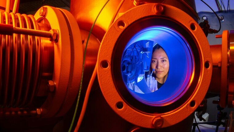
Doctoral candidate Karla Jahaira Paz Corrales experiments with material samples at an ion accelerator. Image: Jens Meyer (University of Jena)
Doctoral candidate Karla Jahaira Paz Corrales experiments with material samples at an ion accelerator. Image: Jens Meyer (University of Jena) - While computer chips are becoming smaller and faster with every passing year, there is one challenge that remains unsolved: integrating electronics and photonics onto a single chip. Although micro-LEDs exist as single chips and waveguides as tiny fibre optic cables, the materials required to make them are too heterogenous to combine in a single harmonious chip. A novel etching technique, however, could prove to be the decisive breakthrough in combining optoelectronic light sources and photonic fibre optics. Researchers at Friedrich Schiller University Jena and Technische Universität Braunschweig have launched a joint project focusing on porous gallium nitride. The OptoGaN project-full title "Highly integrated microphotonic modules in nitride technologies"-has been awarded roughly 600,000 euros of funding by the Federal Ministry of Education and Research (BMBF) for a three-year term. Germany's burgeoning photonics industry would be well advised to pay particularly close attention to developments in Jena and Braunschweig in the years ahead. The research groups participating in the project are convinced that their idea could serve an array of potential applications. The project partners hope to establish three applications with one start-up each as demonstrators. Their research could benefit technologies such as waveguides, neuromorphic computing and the trapped-ion quantum computer operated by the Quantum Valley Lower Saxony network. But how exactly might this technology be applied?
TO READ THIS ARTICLE, CREATE YOUR ACCOUNT
And extend your reading, free of charge and with no commitment.